This article has been reviewed according to Science X's editorial process and policies. Editors have highlighted the following attributes while ensuring the content's credibility:
fact-checked
proofread
Fundamental and photodetector application of van der Waals Schottky junctions

The junction composed of traditional metals and 2D semiconductors is a key component of semiconductor devices.
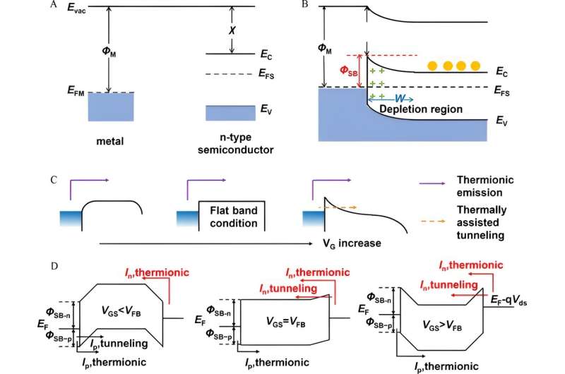
Ideally, Schottky barrier height (SBH) can be obtained based on the relative alignment of energy levels according to the Schottky-Mott rule. However, the Schottky-Mott rule was invalid due to the Fermi level pinning (FLP) effect, it is difficult to tune SBH by changing the work function of metals. The precise design and modulation of SBH is challenging and the issue of FLP should be addressed.
In this review, the authors summarized the fundamental concept of vdW Schottky junction, including the band alignment at the interface and the SBH extraction models. Then the origins of FLP and the strategies to eliminate FLP were introduced.
In terms of 2D surface contact, inserting buffer layer, vdW contact with 3D metal by dry transfer method and constructing all 2D vdW contact using semimetallic 2D materials were introduced respectively to minimize SBH.
Meanwhile, 1D edge contact by etching or phase transition can also realize Fermi level depinning. On the basis of 2D vdW Schottky junctions which can effectively restrain the FLP effect, modulation of the Schottky barrier via external field, such as electrostatic gating and ferroelectric polarization and strain, were further introduced.
The research is published in the journal Advanced Devices & Instrumentation.
The recent development of photodetectors based on 2D Schottky junctions were then summarized, which show the characteristics of high sensitivity, self-driven operation and fast response. Compared with conventional bulk Schottky junction photodetector, the 2D Schottky junction device is expected to possess lower dark current.
Moreover, all-2D vdW junctions employing semimetallic 2D materials exhibited higher energy conversion efficiency and efficient control of Schottky barrier due to the eliminated FLP. The tunability of Schottky junctions also enabled the realization of reconfigurable photodiode, which is beneficial for multifunctional photodetection.
The authors further summarized the strategies for improving photodetection based on vdW Schottky junction from the aspects of enhanced optical absorption, extended wavelength range, increased photogain and design of anisotropic 2D metal.
Schottky junctions have important application aspects in the field of photodetection. However, the poor rectifying and uncontrolled carrier transport characteristic in 2D Schottky junctions restrict its application, attributing to the strong FLP effect.
Different kinds of 2D semimetals offer abundant choices for the design of vdW Schottky junction based on the work function of 2D metals according to the Schottky-Mott rule. The Fermi levels of 2D metals can be easily modulated, enabling the flexible tuning of SBH, which is essential for realizing the full potential of 2D Schottky junctions and further improving the photodetection performance.
The future directions can be focus on the fabrication of large-scale vdW Schottky junction, flexible modulation of Schottky barrier width and mechanisms of tunable hot-electron photodetection.
More information: Jing-Yuan Wu et al, Fundamental and Photodetector Application of Van Der Waals Schottky Junctions, Advanced Devices & Instrumentation (2023). DOI: 10.34133/adi.0022
Provided by Advanced Devices & Instrumentation


