CERN Accélérateur de science

 
: aboveskip=-1pt,belowskip=-1pt
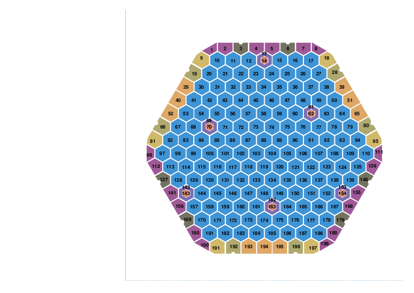
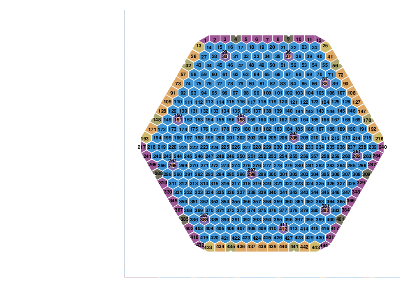
: Layout of the tested 8'' prototype silicon pad sensors with (a) the low-density (LD) and (b) the high-density (HD) design. Regular-sized hexagonal pads are depicted in cyan. Edge and corner pads populate the sensor periphery. Six (LD), respectively twelve (HD), regular, small hexagonal pads on the sensor are dedicated for energy calibration with minimum ionising particles up to the end of life. The colour coding highlights the usage of different pad geometries. The sensor guard rings are not shown.
(a) Schematic of the beam port sample delivery system at RINSC. (b) The view into the beam port used for these irradiation studies. (c) The sample delivery cylinder that contains the sensor-holding hockey pucks and (d) dry ice for cooling of the silicon sensors in the beam port during and after irradiation.
(a) Sample containers ('hockey puck') designed to hold CE silicon sensors for neutron irradiation at RINSC. Wood (oak), acrylic, and PEEK were the puck materials that were experimented with. (b) An 8'' high-density CE prototype silicon sensor inside an acrylic puck covered with a Kapton\texttrademark$~$foil.
Representative temperature recordings during two of the RINSC irradiation rounds of CE prototype silicon sensors. The time when the irradiation was started and when it ended is indicated. The increase of the temperature towards its plateau coincides with the sublimation of the dry ice inside the delivery cylinder.
A low-density CE silicon pad sensor right before connecting to the switch- and probe-card ARRAY system at CERN. The probe station was closed and continuously flushed with dry air during the testing to prevent the formation of ice during low-temperature operation.
: aboveskip=-1pt,belowskip=-1pt
: (a) Total leakage currents after irradiation (without additional thermal annealing) for two representative example sensors. Currents were measured at \SI{-40}{\celsius} ($\text{I}_\text{tot, \SI{-40}{\celsius}}$) and at different effective bias voltages ($\text{U}_\text{bias}$). (b) Per-pad leakage currents normalised to the area of full hexagonal pads as a function of the bias voltage for different pads with different geometries on one example sensor.
: aboveskip=-1pt,belowskip=-1pt
: (a) IV-curves of a representative full hexagonal pad for different annealing durations for a \SI{200}{\micro\metre} low-density prototype sensor irradiated to approximately 2.4$\times 10^{15}~\neqcm$. (b) Decrease of the per-pad leakage current ($U_\text{bias}=\SI{600}{\volt}$) as a function of the annealing time ($\text{t}_\text{annealing}$) at \SI{60}{\celsius}.
aboveskip=-1pt,belowskip=-1pt : Volume-normalised per-pad leakage currents interpolated to an effective bias voltage of \SI{600}{\volt} as a function of the fluence that they were exposed to. The quoted currents were measured after additional annealing at \SI{60}{\celsius}, and are scaled to the CE's planned operation temperature of \SI{-30}{\celsius}. "0.5x p-stop" denotes HD sensors with half the p-stop concentration. "TTU" denotes the measurements of \SI{120}{\micro\meter} HD sensors conducted with a analogous setup to the one described in~\ref{subsec:setup_alps}, at Texas Tech University. Those exhibit overall consistency with the measurements conducted at CERN.
: aboveskip=-1pt,belowskip=-1pt
: Per-pad leakage currents interpolated to an effective bias voltage of \SI{600}{\volt} for three representative sensors from different irradiation rounds before (a-c) and after additional annealing (d-f). Red- or white-colored edge pads correspond to well-understood measurement effects, e.g. insufficient contact between the pogo pins and the pads.
: Caption not extracted
: aboveskip=-1pt,belowskip=-1pt
: (a) Reciprocal-squared capacitance ($C^{-2}_\text{pad}$) as a function the bias voltage of a representative full hexagonal pad for different annealing durations for a \SI{200}{\micro\metre} low-density prototype sensor irradiated to approximately 2.4$\times 10^{15}~\neqcm$. (b) Relative decrease of the depletion voltage estimate ($U_\text{dep}$) as a function of the additional annealing time ($\text{t}_\text{annealing}$) at \SI{60}{\celsius} for a subset of full pads.
: aboveskip=-1pt,belowskip=-1pt
: (a) Area-normalised capacitances as a function of the bias voltage for different pads with different geometries on a example LD sensor. (b) Normalised squared-inverse capacitances as a function of the bias voltage to estimate the sensor depletion voltage of a central pad from different irradiation rounds. Full depletion was achieved at bias voltages around \SI{40}{\volt} for \SI{120}{\micro\metre} sensors, \SI{120}{\volt} for \SI{200}{\micro\metre} sensors, and \SI{280}{\volt} for the \SI{300}{\micro\meter} sensors before irradiation.
: aboveskip=-1pt,belowskip=-1pt
: (a) Per-pad depletion voltage estimates for a \SI{200}{\micron} LD example sensor irradiated to 1.9$\times 10^{15}~\neqcm$, and (b) their correlation to the per-pad leakage current, used as proxy for the delivered fluence.
Leakage currents as a function of the bias voltage for an example sensor measured at \SI{-40}{\celsius}, \SI{-35}{\celsius}, \SI{-30}{\celsius}, and scaled to \SI{-35}{\celsius} using$~$\ref{eq:temp_scaling}.
: aboveskip=-1pt,belowskip=-1pt
: (a) Temperature differences derived from per-pad leakage currents between symmetric locations of a representative neutron-irradiated CE silicon sensors on the cold chuck at CERN. (b) Determined profile of temperature differences, modelled as a two-dimensional gaussian, across the sensor surface. (c) Closure check: derived temperature differences after accordingly correcting the measured per-pad leakage currents.
: Caption not extracted